|
 |
|
| Wafer Surface Analyzer |
 |
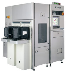 |
| WM-5000 |
|
 |
World only Violet Laser Diode for
light source |
|
Both the maximum detectivity of 0.041microns
and a wide dynamic range (from 0.041 to 5microns)
are attained. |
|
Newly developed optics "Maps"(Multi-beam & Polarize
OpticalSystem) offers optimum
detection of new materials such as High-k, Low-K,
SOI, SiGe, etc. |
|
Substantially improved coordinate accuracy
has reduced the working time on the review SEM. |
|
Supporting mini-environments (SMIF/FOUP) |
|
A high-precision edge grip mechanism
is optionally available, which can minimize the contamination
on the wafer. |
|
Double-sided measurement is available
by installing the optional wafer backside measurement
function |
|
<Major specifications>
| Light source |
Violet Laser Diode |
| Detecting/scanning
method |
Scattered light detecting / helical scanning
method |
| Detectivity |
Bare 0.041microns / film 0.061microns |
| Dynamic range |
0.041microns to 5microns |
| Reproducibility |
| σn / |
 |
≦1% |
|
| Wafer size |
300/200mm, 200/150 mm |
| Throughput |
100 wafers/h (200 mm) |
| X/Y coordinate
reproducibility |
3σ≦ 20
microns |
| Measurement
availability |
Bare wafer / wafer with film |
| Floor space
to be occupied |
1410(W) X 1685(D) |
| Size (mm) |
1410(W) X 1685(D) X 1920(H) |
| Weight (kg) |
1,200 |
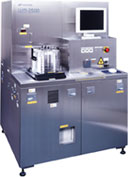
| Wafer Surface
Analyzer WM-3000FOUP/3000/2500SMIF/2500 |
 |
| WM-3000FOUP |
|
|
Both the maximum detectivity of 0.055microns
and a wide dynamic range (from 0.055 to 5microns)
are attained. |
|
Every kind of film such as Cu is supported,
and microscratch and COP separate measurement are
possible. |
|
Substantially improved coordinate accuracy
has reduced the working time on the review SEM. |
|
Supporting mini-environments (WM-2500SMIF/WM-3000FOUP) |
|
A high-precision edge grip mechanism
is optionally available, which can minimize the contamination
on the wafer. |
|
Double-sided measurement is available
by installing the optional wafer backside measurement
function. |
|
 |
 |
 |
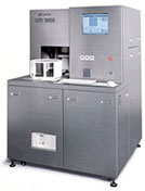
| WM-3000 |
WM-2500SMIF |
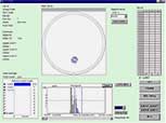
Sample measurement screen |
<Major specifications>
| |
WM-3000FOUP |
WM-3000 |
WM-2500SMIF |
WM-2500 |
| Light
source |
Argon ion laser |
| Detecting/scanning
method |
Scattered
light detecting / helical scanning method |
| Detectivity |
Bare 0.055 microns
/ film 0.07 microns |
| Dynamic
range |
0.055 microns
to 5 microns |
| Reproducibility |
| σn / |
|
≦1% |
|
| Wafer
size |
300/200 mm |
200/150 mm |
| Throughput |
55 wafers/h(300
mm) |
70 wafers/h(200
mm) |
X/Y coordinate
reproducibility |
3σ ≦ 30
microns |
Measurement
availability |
Bare wafer /
wafer with film |
Floor
space to be
occupied |
1,260(W) X 1,685(D) |
1,150(W) X 1,120(D) |
1,200(W) X 1,220(D) |
1,150(W) X 1,120(D) |
| Size (mm) |
1,260(W) X 1,685(D)
X 1,820(H) |
1,150(W) X 1,120(D)
X 1,620(H) |
1,200(W) X 1,220(D)
X 1,670(H) |
1,150(W) X 1,120(D)
X 1,620(H) |
| Weight
(kg) |
1,200 |
800 |
800 |
800 |
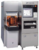
| Wafer Surface
Analyzer WM-7 |
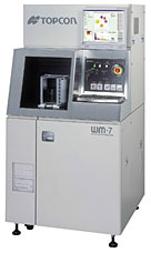 |
| WM-7 |
|
|
Violet Laser Diode installed reducing
the running costs drastically |
|
Wafer handling system even applicable
to III/V compound/new materials |
|
Supporting wafers of various sizes
(ranging from 50 mm to 200 mm) |
|
High performance, low price, easy operation,
and space-saving |
|
Particle information with higher accuracy
provided via real-time counting process |
|
<Major specifications>
| Light source |
Violet LD |
| Detecting/scanning
method |
Scattered light detecting / helical scanning
method |
| Detectivity |
Bare 0.09 microns/ film 0.13 microns |
| Dynamic
range |
0.09 microns to 5 microns |
| Reproducibility |
| σn / |
|
≦1% |
|
| Wafer
size |
200/150/125 mm, 150/125/100 mm
125/100/76 mm, 76/50 mm |
| Throughput |
60 wafers/h (200 mm) |
| X/Y
coordinate reproducibility |
3σ≦ 50
microns |
| Measurement
availability |
Bare wafer / wafer with film / glass
substrate |
| Floor
space to be occupied |
860(W) X 900(D) |
| Size
(mm) |
860(W) X 900(D) X 1,650(H) |
| Weight
(kg) |
600 |
|